Design Automation for Analog Circuits
Contact: Helmut Graeb, Markus Leibl
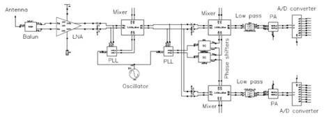
Analog and mixed-signal circuits like, e.g., operational amplifiers, filters, sense amplifiers, low-noise amplifiers, phase-locked loops, A/D-converters, mixers, analog receiver front ends, are vital parts of any integrated system. Although on average taking only 20 percent of the chip area, analog components require about 40 percent of the design effort and cause 50 percent of the design errors discovered after first silicon. Analog design is particularly difficult: it deals with a huge number of specific circuit classes, it requires a customized design approach for each circuit class, and analog circuits are very susceptible to noise and variations. No wonder that analog design automation is particularly difficult as well. Current research projects are:
Structure Analysis and Design
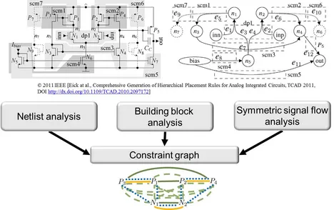
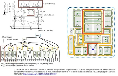
Based on the circuit specification, the definition of the operating principle of the circuit under design and its structure have to be designed. Circuit structure comprises a set of devices, e.g., transistors, and their connection through signal connections. The circuit structure often is given in form of a schematic or a netlist, and comprises basic building blocks like current mirrors, which in turn entail a certain signal flow. Automatic analysis of the inherent building block hierarchy and its corresponding signal flow is crucial for analog design automation.
Circuit Sizing for Yield and Reliability
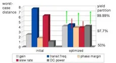
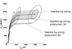
In analog design, circuit elements are parameterized. The parameters of each circuit under design have to be furnished with values, a so-called sizing. Examples are widths or lengths of the transistor’s channels, or capacitances. Frequently, discrete parameters have to be incorporated, e.g., to fit to a manufacturing grid or to size a rectangular-shaped inductor. Nominal design aims at optimizing the nominal performance values of a circuit by systematic tuning of circuit parameters. Tolerance design additionally considers manufacturing variations, varying operating conditions, and aging. Worst-case distances have been proposed as a key reliability measure for tolerance design. Other tasks in circuit sizing is to consider all possible trade-offs by means of Pareto optimization and to consider the layout effects.
Layout Synthesis
Once, the circuit structure and sizing are ready, the layout has to be designed. The layout represents the blueprint of the geometric shapes of the physical implementation of the circuit as integrated circuit, i.e., chip. Layout comprises placement, i.e., the positions and shapes of the devices on the chip, and routing, i.e. the routes and shapes of the signal interconnects.
